Last post we present the XV-J550 and XV-T550 video titlers. One is targeted to Japanese market and the other to western markets, this difference reflects in some changes between both models. Being a video titler, XV-J550's main function is to put text on screen, since it's aimed for Japanese market, it needs to support Kanji characters, so it have, at least, more ROM than XV-T550, to store these Kanji Fonts.
Although they have the same outward appearance, XV-J550 and XV-T550 have different PCBs. Evidence suggests that the XV-T550's PCB was prepared to be shared with the XV-J550, there are some unpopulated placements for ROM on XV-T550's mainboard that can be used by Kanji ROM.
 |
| This is the mainboard from XV-T550, take a look in the two unpopulated placements for ROM chips and the shielding over V9938 (picture from this MSX Village thread) |
By now, all (three) XV-J550 that I saw the insides had the same PCB's look (maybe different minor revisions, but the same overall shape). And this PCB's appearance is consistently different from the one that I saw in pictures of XV-T550 and is printed in its service manual:
 |
| This is the XV-J550 mainboard seen from solder side. The two chips that you can see are the Sony custom mapper and the MSX-System II |
 |
| And this is the XV-T550 mainboard, picture from XV-T550 Service Manual. You can see that many components are in different locations on the board. |
My guess: the XV-J550 was first released in Japan. Seeing that it's a good product and there is a broader home video market, Sony wanted to sell it in Europe, but had to make some revisions on the board for this release; this new board was meant to be shared by the two versions of the titler (XV-J550 and XV-T550), but for some reason the XV-J550 with the new PCB did not reached the market (or we didn't yet found any XV-J550 with this new board). I believe that, instead release the same old product with a new internal organisation, Sony did launched new video titlers, like the XV-J770.
What's inside XV-J550?
There is two big boards (and some small boards) in XV-J550. One with all the MSX hardware and other responsible to handle the AV inputs and outputs. The designers made a very compact unit, the other video titlers from Sony have almost two times the height of the XV-J550/XV-T550:
 |
| XV-J550 on top of XV-J777. |
This compactness made the XV-J550 a beautiful equipment, but compromises the "hacking" possibilities. It's impossible to use the cartridge slot while XV-J550 is closed and is very hard to fit any additional circuitry in this limited space.
 |
| How you can use the XV-J550/XV-T550 cartridge slot |
XV-J550 have most of what can be expected from a MSX2 system, but it have only one joystick port, one MSX slot and the keyboard connector doesn't have all pins connected to use a complete MSX keyboard.
CPU: Z80 @ 3.58Mhz
RAM: 64KB
VDP: Yamaha V9938 with 128KB VRAM
PPI: MSX-System II
Sound: PSG equivalent inside MSX-System II
Storage: 64KB SRAM energized by a CR2032 battery
Keyboard: separated keyboard customized for video production functions
Additional features: Superimposer
I/O ports: two stereo AV inputs and two stereo AV outputs, one keyboard connector, one joystick port and one MSX slot.
There is no external storage in XV-J550, but you can save your title sequences in the battery backed SRAM. The MSX slot lacks some pins too, namely: +12/-12 volts, SOUNDIN, SW1, SW2 and BUSDIR.
Without the RAM and ROM chips, the main ICs on processor board are:
Oki M71H003: Unknown
Sharp LH0080A: Z80 compatible
Sony MB64H444:Custom memory mapper
Yamaha S1985: MSX-SYSTEM II
Yamaha V9938: Video Display Processor
 |
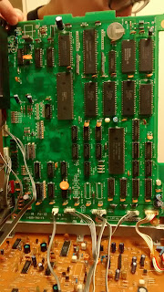
| Here you can see the Z80, the mysterious OKI chip and some RAMs and ROMs. You can't see the slot connector because there is a MegaFlashROMSCC+SD 512 connected there. |
 |
| The V9938 and the 128KB VRAM |
 |
| MSX-System II from Yamaha |
 |
| Sony custom mapper. Probably a Fujitsu MB64H444PF gate array |
There is many ROM chips on this circuit board, but I still don't know what is in each one of those. This mystery will be solved when we read the contents of those ROMs in a EPROM reader. Since the Sony HB-F1XD uses the same set of S1985+MB64H444, I won't be surprised if the BIOS and SUB-ROM are also the same in the XV-J550 and HB-F1XD.
The encoder board have a more sparse look and, as said before, handles the AV inputs and outputs. There is only one IC on the backside of this circuit board.
 |
| The "other" board |
 |
| The lonely IC on "other" board backside: SONY D1030 |
I did not found the usual SONY V70X0 chips inside the XV-J550, they are very common on MSX2 machines that have digitizer and/or superimposer features. But there are a lot of "washed" chips on the encoder board, any of those chips can be a V70X0 IC, so we can't really say that this machine hasn't the Sony video chipset.
Next post, more Sony video equipment!


No comments:
Post a Comment